
By Alua Suleimenova, Senior Sustainability Program Manager, Marvell

This blog was originally posted in Semiconductor Engineering.
The semiconductor industry is the bedrock of modern technology, enabling everything from AI and cloud computing to electric vehicles. Yet, this critical sector is also one of the most resource-intensive globally, with a substantial dependency on water. A single fabrication plant can demand up to 10 million gallons of water daily, comparable to the consumption of a city with 300,000 residents. Much of this water is, of course, reused and recycled through sophisticated systems. This immense water usage, particularly the requirement for ultrapure water for processes like cleaning and etching, makes consistent access to high-quality water a non-negotiable for operational reliability and business continuity. The new insights report “Ripple Effects: Water Risk and Resilience Across the Semiconductor Value Chain” provides the first global baseline of water risk hotspots for the semiconductor sector, assessing water risks across 140 facilities across 89 water basins to inform future risk mitigation strategies.
By Khurram Malik, Senior Director of Marketing, Custom Cloud Solutions, Marvell
Can AI beat a human at the game of twenty questions? Yes.
And can a server enhanced by CXL beat an AI server without it? Yes, and by a wide margin.
While CXL technology was originally developed for general-purpose cloud servers, the technology is now finding a home in AI as a vehicle for economically and efficiently boosting the performance of AI infrastructure. To this end, Marvell has been conducting benchmark tests on different AI use cases.
In December, Marvell, Samsung and Liqid showed how Marvell® StructeraTM A CXL compute accelerators can reduce the time required for conducting vector searches (for analyzing unstructured data within documents) by more than 5x.
In February, Marvell showed how a trio of Structera A CXL compute accelerators can process more queries per second than a cutting-edge server CPU and at a lower latency while leaving the host CPU open for different computing tasks.
Today, this blog post will show how Structera CXL memory expanders can boost performance of inference tasks.
By Khurram Malik, Senior Director of Marketing, Custom Cloud Solutions, Marvell
While CXL technology was originally developed for general-purpose cloud servers, it is now emerging as a key enabler for boosting the performance and ROI of AI infrastructure.
The logic is straightforward. Training and inference require rapid access to massive amounts of data. However, the memory channels on today’s XPUs and CPUs struggle to keep pace, creating the so-called “memory wall” that slows processing. CXL breaks this bottleneck by leveraging available PCIe ports to deliver additional memory bandwidth, expand memory capacity and, in some cases, integrate near-memory processors. As an added advantage, CXL provides these benefits at a lower cost and lower power profile than the usual way of adding more processors.
To showcase these benefits, Marvell conducted benchmark tests across multiple use cases to demonstrate how CXL technology can elevate AI performance.
By Sandeep Bharathi, president, Data Center Group, Marvell
This blog was originally posted at Fortune.
Semiconductors have transformed virtually every aspect of our lives. Now, the semiconductor industry is on the verge of a profound transformation itself.
Customized silicon—chips uniquely tailored to meet the performance and power requirements of an individual customer for a particular use case—will increasingly become pervasive as data center operators and AI developers seek to harness the power of AI. Expanded educational opportunities, better decision making, ways to improve the sustainability of the planet all become possible if we get the computational infrastructure right.
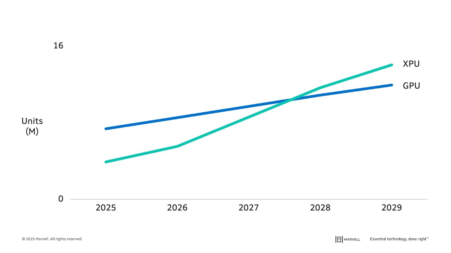
The turn to custom, in fact, is already underway. The number of GPUs—the merchant chips employed for AI training and inference—produced today is nearly double the number of custom XPUs built for the same tasks. By 2028, custom accelerators will likely pass GPUs in units shipped, with the gap expected to grow.1
By Michael Kanellos, Head of Influencer Relations, Marvell
Chiplets—devices made up of smaller, specialized cores linked together to function like a unified device—have dramatically transformed semiconductors over the past decade. Here’s a quick overview of their history and where the design concept goes next.
1. Initially, they went by the name RAMP
In 2006, Dave Patterson, the storied professor of computer science at UC Berkeley, and his lab published a paper describing how semiconductors will shift from monolithic silicon to devices where different dies are connected and combined into a package that, to the rest of the system, acts like a single device.1
While the paper also coined the term chiplet, the Berkeley team preferred RAMP (Research Accelerator for Multiple Processors).
2. In Silicon Valley fashion, the early R&D took place in a garage
Marvell co-founder and former CEO Sehat Sutardja started experimenting with combining different chips into a unified package in the 2010s in his garage, according to journalist Junko Yoshida.2 In 2015, he unveiled the MoChi (Modular Chip) concept, often credited as the first commercial platform for chiplets, in a keynote at ISSCC in February 2015.3
The first products came out a few months later in October.
“The introduction of Marvell’s AP806 MoChi module is the first step in creating a new process that can change the way that the industry designs chips,” wrote Linley Gwennap in Microprocessor Report.4
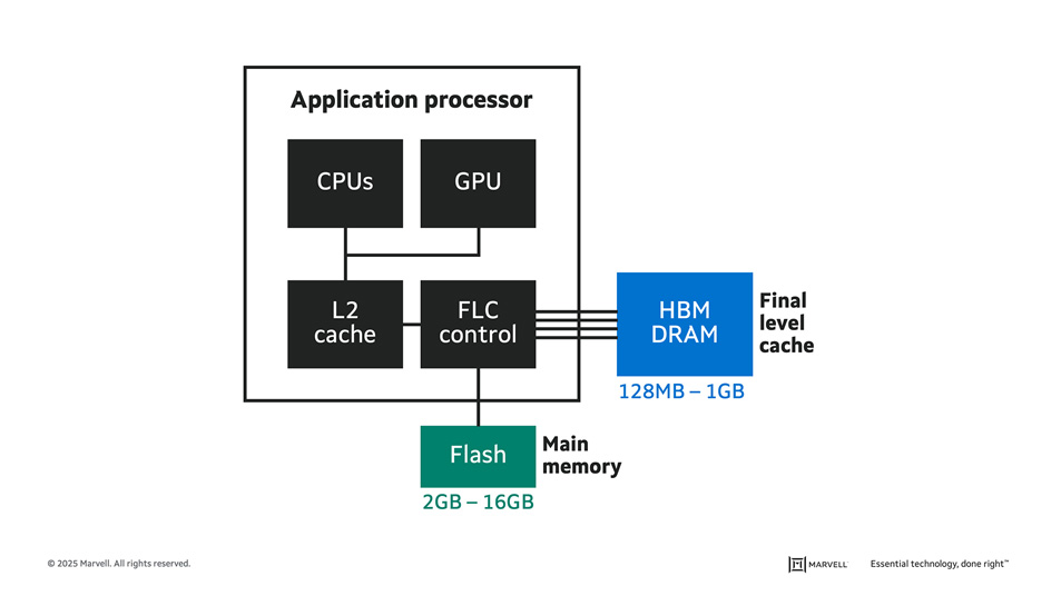
An early MoChi concept combining CPUs, a GPU and a FLC (final level cache) controller for distributing data across flash and DRAM for optimizing power. Credit: Microprocessor Forum.