This article was first published in Photonic Integrated Circuits magazine.
The dominant challenge in modern AI infrastructure is not just the performance of a single accelerator but scaling up to thousands of accelerators (XPUs) in a cluster. Training and inference workloads now depend on an interconnect that can stitch these accelerators into a high-bandwidth, low-latency system, where performance is governed as much by the network as by the compute itself.
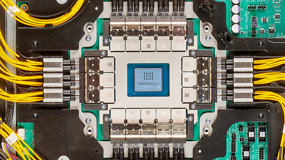
As these systems scale, physics asserts itself. Electrical links over copper hit a practical ceiling as routing density and channel loss collide, turning the loss bandwidth product into an impassable constraint. The choice is binary: either move electrical-to-optical conversion closer to the Application-Specific Integrated Circuit (ASIC) or surrender the link budget. Thus, to bypass this electrical wall, optics must migrate from the board edge and onto the ASIC package.
This progression is not an architectural preference; it is a physical necessity. Every serious scale-up roadmap eventually converges on the same outcome: optical interfaces migrating from front-panel modules (including optical-engine-based pluggables) to Near-Packaged Optics (NPO), and ultimately to Co-Packaged Optics (CPO) integrated alongside the compute die. CPO is not the goal in itself, but the inevitable consequence of interconnect bandwidth scaling.
The bottleneck moves to test
Silicon photonics platforms today deliver extraordinary functionality and bandwidth density, but the industry is hitting a manufacturing wall. Historically, optical testing has evolved as a specialized, low-volume practice. Test cells are often custom-built, alignment-heavy, and single-site. Optical instruments typically reside outside the Automated Test Equipment (ATE) ecosystem in rack-and-stack configurations, and throughput is measured in minutes rather than seconds. While these approaches suffice for labs and pilot lines, they break down at high channel counts and production volumes.
The issue is not the measurement rigor; it’s manufacturing efficiency at scale. As optics move inward toward the ASIC, we still need the same level of test coverage, but delivered with IC-style parallelism, repeatability, and automation.
For the rest of the article, please go to Photonic Integrated Circuits.
# # #
This blog contains forward-looking statements within the meaning of the federal securities laws that involve risks and uncertainties. Forward-looking statements include, without limitation, any statement that may predict, forecast, indicate or imply future events or achievements. Actual events or results may differ materially from those contemplated in this blog. Forward-looking statements are only predictions and are subject to risks, uncertainties and assumptions that are difficult to predict, including those described in the “Risk Factors” section of our Annual Reports on Form 10-K, Quarterly Reports on Form 10-Q and other documents filed by us from time to time with the SEC. Forward-looking statements speak only as of the date they are made. Readers are cautioned not to put undue reliance on forward-looking statements, and no person assumes any obligation to update or revise any such forward-looking statements, whether as a result of new information, future events or otherwise.
Tags: AI infrastructure, Optical Interconnect, Optical DSPs, DSP, data center interconnect, hyperscale data center networks, Optical Connectivity, AI
Copyright © 2026 Marvell, All rights reserved.