
Just like its civilian counterparts, the government uses semiconductors to enable all critical systems. Moreso than its civilian counterparts, the government uses semiconductors for system which can expose those semiconductors to extreme conditions and in addition have highly stringent requirements for security. With lives, safety, and national security on the line, the government can’t afford for these chips to fail.
As demand for chips that meet government specs increases, so do the costs associated with developing these highly technical and specific chips, particularly as the government works to integrate rapidly developing applications, such as artificial intelligence (AI).
But here’s the problem: chips that meet the government’s stringent specifications cannot be developed in a day, so by the time they complete what can be a long development and testing process, they may be eclipsed by newer technology.
So how can the government get the advanced chips they need and get them quickly enough to keep up with ever-changing technology?
By taking a dual-use approach to the problem, Marvell Government Solutions is extending the specs of our market-tested intellectual property (IP) and optimizing it for government-specific use cases—saving time and costs while leveraging our experience in design, supply chain management, advanced testing, and manufacturability. Here’s how.
Finding answers in existing technology
In mid-2021, a government entity approached Marvell because one of its designs was not meeting the environmental specifications. They had worked with another design house for two years to develop the IP to enable this chip to run at -55 C. Unfortunately, once the design was implemented in silicon, it did not meet the specifications for the application.
Rather than taking two more years to develop a completely new IP block, we instead turned to our existing IP portfolio. We identified a piece of IP that was being used in another design that could be altered to meet specs. We believed we could remove the nonconforming design from the government’s primary chip and replace it with our IP. While our existing silicon technology had not been designed to withstand the government’s temperature requirements, we immediately began working with one of our design teams to enable the IP to work in the extended temperature range.

Caption: While our IP did not natively meet the -55 C requirement, we believed we could modify the technology to withstand the required temperature extremes.
From two years to six months
We explored the possibility of creating a dual-use piece of analog IP that could be used in multiple markets and applications by expanding the temperature range for from -40 C to +125 C to -55 C to +125 C. We also modified the Phase Locked Loop—one of the critical building blocks—to make it low-jitter. We were able to complete the design work in six months and get models to the chip design team so they could work on integrating the IP into the custom design for the government.
The IP and chip development tracks were done in parallel—the IP team was characterizing the analog IP while the chip design team was completing the chip design. This significantly reduced the overall project length, minimizing the delay due to the old analog IP block.
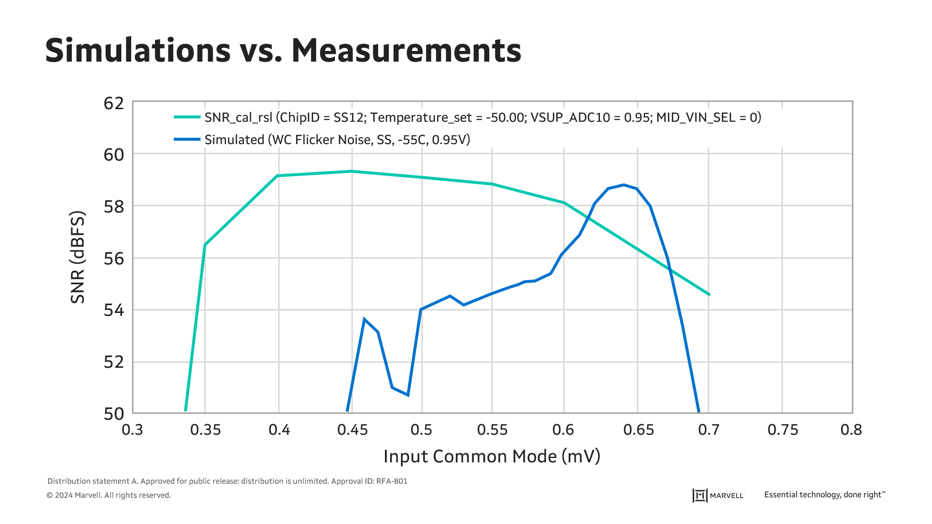
Once the IP test chip silicon was received, tests showed degradation at lower temperatures. This behavior was not observed in simulations, so some detective work was required to identify root-cause and modify the design so that it met the cold corner temperature spec. The analog IP was successfully redesigned and verified before the chip design was completed, and the changes did not require the chip models to be modified.
In just six months, we gave the government models that would enable them to design the bigger chip, saving them massive amounts of development time and money. This design is currently being released as a government product and is in manufacturing.
The bigger picture
In the world of technology, efficiency is often imperative given the rapid pace of change. While it can certainly make sense to develop a new solution from scratch, the length of the development cycle can render a solution uncompetitive by the time it comes to market. Especially when it comes to sensitive analog IP, it is necessary to plan for multiple iterations to ensure that specifications are met.
At Marvell, we’ve worked to continuously extend the architecture of our IP, building on the solid foundation of tried and tested designs. Not only does this methodology allow us to improve resolution and performance while upholding security standards but allows our government customers to reap the benefits faster, without multi-year development periods.
The best part? This applies to our entire product catalog. From 5G or 6G processors to PHYs and DSPs, we can elaborate on our existing designs to meet government specifications, saving money and time by reusing proven designs.
Learn more about Marvell Government Solutions here.
# # #
This blog contains forward-looking statements within the meaning of the federal securities laws that involve risks and uncertainties. Forward-looking statements include, without limitation, any statement that may predict, forecast, indicate or imply future events or achievements. Actual events or results may differ materially from those contemplated in this blog. Forward-looking statements are only predictions and are subject to risks, uncertainties and assumptions that are difficult to predict, including those described in the “Risk Factors” section of our Annual Reports on Form 10-K, Quarterly Reports on Form 10-Q and other documents filed by us from time to time with the SEC. Forward-looking statements speak only as of the date they are made. Readers are cautioned not to put undue reliance on forward-looking statements, and no person assumes any obligation to update or revise any such forward-looking statements, whether as a result of new information, future events or otherwise.
Tags: MGS
Copyright © 2026 Marvell, All rights reserved.
