
By Michael Kanellos, Head of Influencer Relations, Marvell
The opportunity for custom silicon isn’t just getting larger – it’s becoming more diverse.
At the Custom AI Investor Event, Marvell executives outlined how the push to advance accelerated infrastructure is driving surging demand for custom silicon – reshaping the customer base, product categories and underlying technologies. (Here is a link to the recording and presentation slides.)
Data infrastructure spending is now slated to surpass $1 trillion by 20281 with the Marvell total addressable market (TAM) for data center semiconductors rising to $94 billion by then, 26% larger than the year before. Of that total, $55.4 billion revolves around custom devices for accelerated compute1. In fact, the forecast for every major product segment has risen in the past year, underscoring the growing momentum behind custom silicon.
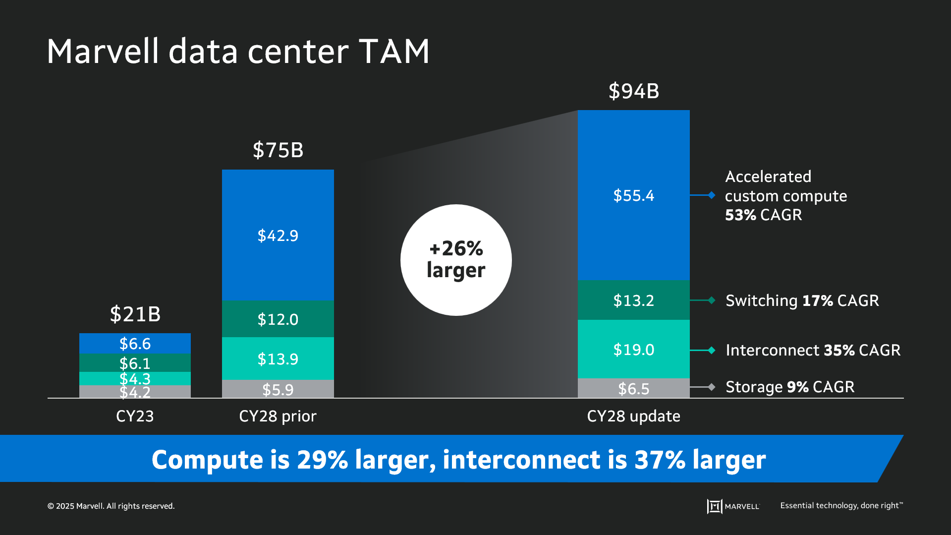
The deeper you go into the numbers, the more compelling the story becomes. The custom market is evolving into two distinct elements: the XPU segment, focused on optimized CPUs and accelerators, and the XPU attach segment that includes PCIe retimers, co-processors, CPO components, CXL controllers and other devices that serve to increase the utilization and performance of the entire system. Meanwhile, the TAM for custom XPUs is expected to reach $40.8 billion by 2028, growing at a 47% CAGR1.
By Michael Kanellos, Head of Influencer Relations, Marvell
You’re likely assaulted daily with some zany and unverifiable AI factoid. By 2027, 93% of AI systems will be able to pass the bar, but limit their practice to simple slip and fall cases! Next-generation training models will consume more energy than all Panera outlets combined! etc. etc.
What can you trust? The stats below. Scouring the internet (and leaning heavily on 16 years of employment in the energy industry) I’ve compiled a list of somewhat credible and relevant stats that provide perspective to the energy challenge.
1. First, the Concerning News: Data Center Demand Could Nearly Triple in a Few Years
Lawrence Livermore National Lab and the Department of Energy1 has issued its latest data center power report and it’s ominous.
Data center power consumption rose from a stable 60-76 terawatt hours (TWh) per year in the U.S. through 2018 to 176 TWh in 2023, or from 1.9% of total power consumption to 4.4%. By 2028, AI could push it to 6.7%-12%. (Lighting consumes 15%2.)
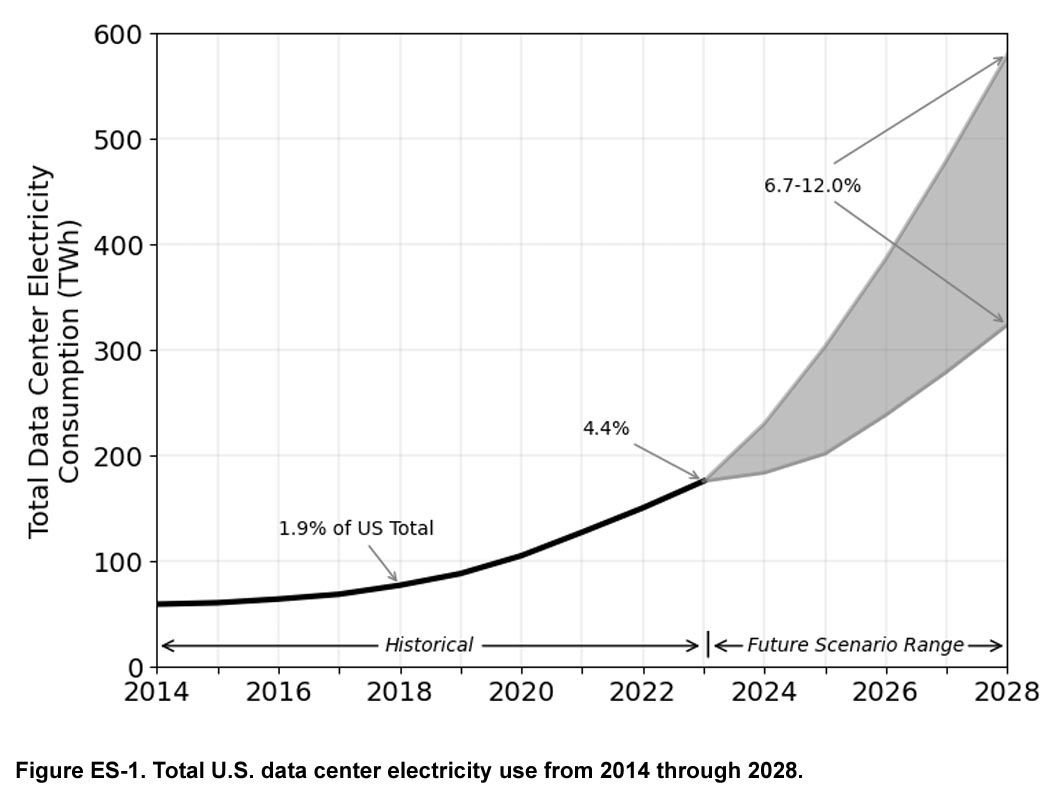
Report co-author Eric Masanet adds that the total doesn’t include bitcoin, which increases 2023’s consumption by 70 TWh. Add a similar 30-40% to subsequent years too if you want.
This article was originally published in VentureBeat.
Artificial intelligence is about to face some serious growing pains.
Demand for AI services is exploding globally. Unfortunately, so is the challenge of delivering those services in an economical and sustainable manner. AI power demand is forecast to grow by 44.7% annually, a surge that will double data center power consumption to 857 terawatt hours in 20281: as a nation today, that would make data centers the sixth largest consumer of electricity, right behind Japan’s2 consumption. It’s an imbalance that threatens the “smaller, cheaper, faster” mantra that has driven every major trend in technology for the last 50 years.
It also doesn’t have to happen. Custom silicon—unique silicon optimized for specific use cases—is already demonstrating how we can continue to increase performance while cutting power even as Moore’s Law fades into history. Custom may account for 25% of AI accelerators (XPUs) by 20283 and that’s just one category of chips going custom.
The Data Infrastructure is the Computer
Jensen Huang’s vision for AI factories is apt. These coming AI data centers will churn at an unrelenting pace 24/7. And, like manufacturing facilities, their ultimate success or failure for service providers will be determined by operational excellence, the two-word phrase that rules manufacturing. Are we consuming more, or less, energy per token than our competitor? Why is mean time to failure rising? What’s the current operational equipment effectiveness (OEE)? In oil and chemicals, the end products sold to customers are indistinguishable commodities. Where they differ is in process design, leveraging distinct combinations of technologies to squeeze out marginal gains.
The same will occur in AI. Cloud operators already are engaged in differentiating their backbone facilities. Some have adopted optical switching to reduce energy and latency. Others have been more aggressive at developing their own custom CPUs. In 2010, the main difference between a million-square-foot hyperscale data center and a data center inside a regional office was size. Both were built around the same core storage devices, servers and switches. Going forward, diversity will rule, and the operators with the lowest cost, least downtime and ability to roll out new differentiating services and applications will become the favorite of businesses and consumers.
The best infrastructure, in short, will win.
The Custom Concept
And the chief way to differentiate infrastructure will be through custom infrastructure that are enabled by custom semiconductors, i.e., chips containing unique IP or features for achieving leapfrog performance for an application. It’s a spectrum ranging from AI accelerators built around distinct, singular design to a merchant chip containing additional custom IP, cores and firmware to optimize it for a particular software environment. While the focus is now primarily on higher value chips such as AI accelerators, every chip will get customized: Meta, for example, recently unveiled a custom NIC, a relatively unsung chip that connects servers to networks, to reduce the impact of downtime.
By Ravindranath C Kanakarajan, Senior Principal Engineer, Switch BU
Marvell has been actively involved with SONiC since its beginning, with many SONiC switches powered by Marvell® ASICs at hyperscalers deployed worldwide. One of Marvell's goal has been to enhance SONiC to address common issues and optimize its performance for large-scale deployments.
The Challenge
Many hackathon projects have focused on improving the monitoring, troubleshooting, debuggability, and testing of SONiC. However, we believe one of the core roles of a network operating system (NOS) is to optimize the use of the hardware data plane (i.e., the NPUs and networking ASICs). As workloads become increasingly more demanding, it becomes crucial to maximize the efficiency of the data plane. Commercial black-box NOS are tailored to specific NPUs/ASICs to achieve optimal performance. SONiC, however, supports a diverse range of NPUs/ASICs, presenting a unique challenge.
We at Marvell have been contributing features to SONiC to ensure optimal use of the underlying networking ASIC resources. Over time, we’ve recognized the need to provide operators with flexibility in utilizing ASIC resources while reducing the platform-specific complexity gradually being introduced into SONiC’s core component, the Orchagent. This approach will help SONiC operators to maintain consistent device configurations even when using devices from different platform vendors.
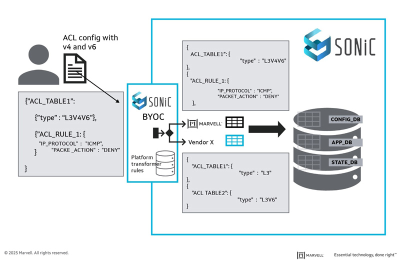
BYOC
During the Hackathon, we developed a framework called “BYOC: Bring Your Own Configuration,” allowing networking ASIC vendors to expose their hardware capabilities in a file describing intent. A new agent transforms the user’s configuration into an optimal SONiC configuration based on the capabilities file. This approach allows ASIC vendors to ensure that user configurations are converted to optimal ASIC configurations. It also allows SONiC operators to fine-tune the hardware resources consumed based on the deployment needs. It further helps in optimally migrating configurations from vendor NOS to SONiC based on the SONiC platform’s capability.
By Michael Kanellos, Head of Influencer Relations, Marvell
How do you get more data to the processor faster?
That has been the central question for computing architects and chip designers since the dawn of the computer age. And it’s taken on even greater urgency with AI. The greater amount of data a processor can access, the more accurate and nuanced the answers will be from the algorithm. Adding more memory, however, can also add cost, latency, and power.
Marvell has pioneered an architecture for custom high-bandwidth memory (HBM) solutions for AI accelerators (XPUs) and will collaborate with Samsung, Micron and SK hynix to bring tailored memory solutions to market. (See comments from Micron, Samsung, SK hynix and Marvell here in the release.)
Customizing the HBM element of XPUs can, among other benefits, increase the amount of memory inside XPUs by 33%, reduce the power consumed by the memory I/O interfaces by over 70%, and free up to 25% of silicon area to add more compute logic, depending on the XPU design1.
The shift—part of the overall trend toward custom XPUs--will have a fundamental and far-reaching impact on the performance, power consumption and design of XPUs. Invented in 2013, HBM consists of vertical stacks of high-speed DRAM sitting on a chip called the HBM base die that controls the I/O interfaces and manages the system. The base die and DRAM chips are connected by metal bumps.
Vertical stacking has effectively allowed chip designers to increase the amount of memory close to the processor for better performance. A scant few years ago, cutting-edge accelerators contained 80GB of HBM2. Next year, the high-water mark will reach 288GB.
Still, the desire for more memory will continue, putting pressure on designers to economize on space, power and cost. HBM currently can account for 25% of the available real estate inside an XPU and 40% of the total cost3. HBM4, the current cutting-edge standard, features an I/O that consists of 32 64-bit channels - an immense size that is already making some aspects of chip packaging extremely complex.
All About Optimizing XPU TCO
The Marvell custom HBM compute architecture involves optimizing the base HBM die and its interfaces, currently designed around standards from JEDEC, with solutions uniquely designed to dovetail with the design, characteristics and performance objectives of the host AI compute die.
Imagine that a hyperscaler wants an AI inference XPU for edge data centers squeezed into dense business districts or urban corridors. Cost and power consumption will be at a premium while absolute compute performance will likely be less important. A custom HBM solution might involve reducing the size of the AI compute die to economize on chip size and power above other considerations.
At the other end of the spectrum, an HBM subsystem for XPUs powering a massive AI training cluster might be tuned for capacity and high bandwidth. In this situation, the emphasis could be on reducing the size of the I/O interface. Reducing I/O size creates space for more interfaces on the so-called beachfront at the side of a chip and hence, boosting total bandwidth.