
How do you get more data to the processor faster?
That has been the central question for computing architects and chip designers since the dawn of the computer age. And it’s taken on even greater urgency with AI. The greater amount of data a processor can access, the more accurate and nuanced the answers will be from the algorithm. Adding more memory, however, can also add cost, latency, and power.
Marvell has pioneered an architecture for custom high-bandwidth memory (HBM) solutions for AI accelerators (XPUs) and will collaborate with Samsung, Micron and SK hynix to bring tailored memory solutions to market. (See comments from Micron, Samsung, SK hynix and Marvell here in the release.)
Customizing the HBM element of XPUs can, among other benefits, increase the amount of memory inside XPUs by 33%, reduce the power consumed by the memory I/O interfaces by over 70%, and free up to 25% of silicon area to add more compute logic, depending on the XPU design1.
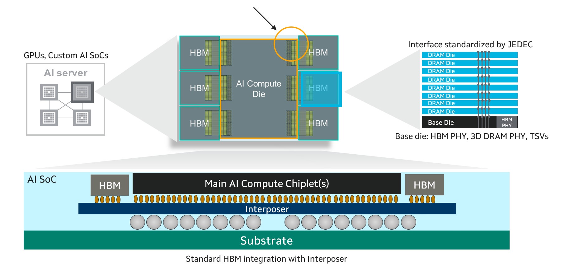
The shift—part of the overall trend toward custom XPUs--will have a fundamental and far-reaching impact on the performance, power consumption and design of XPUs. Invented in 2013, HBM consists of vertical stacks of high-speed DRAM sitting on a chip called the HBM base die that controls the I/O interfaces and manages the system. The base die and DRAM chips are connected by metal bumps.
Vertical stacking has effectively allowed chip designers to increase the amount of memory close to the processor for better performance. A scant few years ago, cutting-edge accelerators contained 80GB of HBM2. Next year, the high-water mark will reach 288GB.
Still, the desire for more memory will continue, putting pressure on designers to economize on space, power and cost. HBM currently can account for 25% of the available real estate inside an XPU and 40% of the total cost3. HBM4, the current cutting-edge standard, features an I/O that consists of 32 64-bit channels - an immense size that is already making some aspects of chip packaging extremely complex.
All About Optimizing XPU TCO
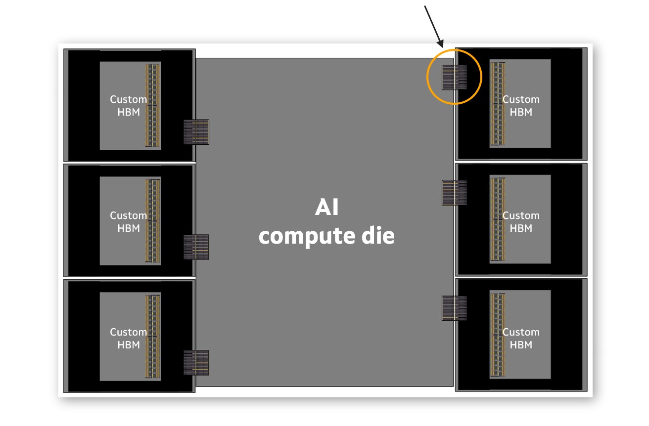
The Marvell custom HBM compute architecture involves optimizing the base HBM die and its interfaces, currently designed around standards from JEDEC, with solutions uniquely designed to dovetail with the design, characteristics and performance objectives of the host AI compute die.
Imagine that a hyperscaler wants an AI inference XPU for edge data centers squeezed into dense business districts or urban corridors. Cost and power consumption will be at a premium while absolute compute performance will likely be less important. A custom HBM solution might involve reducing the size of the AI compute die to economize on chip size and power above other considerations.
At the other end of the spectrum, an HBM subsystem for XPUs powering a massive AI training cluster might be tuned for capacity and high bandwidth. In this situation, the emphasis could be on reducing the size of the I/O interface. Reducing I/O size creates space for more interfaces on the so-called beachfront at the side of a chip and hence, boosting total bandwidth.


Above: A diagram of an XPU with standard HBM. Below, an artist’s rendering of an XPU with custom HBM from Marvell. Note the reduced size of the I/O. This can be accomplished by customizing the controller or PHY that are part of the base die.
Customizing the Future
While customizing HBM opens a new chapter for the memory industry, it’s part of one of the industry’s largest trends. Custom compute design is already being widely embraced across the industry as the heir to Moore’s Law for advancing performance. The four largest hyperscale data providers have each incorporated custom devices into their infrastructure or announced plans to do so. We estimate that 25% of the market for accelerated infrastructure compute silicon market will be custom by 2028. Customization is also extending beyond XPUs and CPUs to CXL controllers, NICs and other devices. Over the next decade, more sockets, more customers and more classes of devices will follow the same route.
The benefits of custom HBM will have ripple effects across infrastructure. Memory consumes 25-40% of data center power by some estimates4 and future AI clusters are expected to contain 100,000 or more XPUs.
A holistic approach to custom silicon which involves examining every subsystem for potential optimization will play a pivotal role in ensuring AI can become a sustainable and economical phenomenon.
1. Marvell
2. Trendforce.
3. Marvell estimates.
This blog contains forward-looking statements within the meaning of the federal securities laws that involve risks and uncertainties. Forward-looking statements include, without limitation, any statement that may predict, forecast, indicate or imply future events or achievements. Actual events or results may differ materially from those contemplated in this article. Forward-looking statements are only predictions and are subject to risks, uncertainties and assumptions that are difficult to predict, including those described in the “Risk Factors” section of our Annual Reports on Form 10-K, Quarterly Reports on Form 10-Q and other documents filed by us from time to time with the SEC. Forward-looking statements speak only as of the date they are made. Readers are cautioned not to put undue reliance on forward-looking statements, and no person assumes any obligation to update or revise any such forward-looking statements, whether as a result of new information, future events or otherwise.
Tags: AI
Copyright © 2026 Marvell, All rights reserved.
