
The continued evolution of 5G wireless infrastructure and high-performance networking is driving the semiconductor industry to unprecedented technological innovations, signaling the end of traditional scaling on Single-Chip Module (SCM) packaging. With the move to 5nm process technology and beyond, 50T Switches, 112G SerDes and other silicon design thresholds, it seems that we may have finally met the end of the road for Moore’s Law.1 The remarkable and stringent requirements coming down the pipe for next-generation wireless, compute and networking products have all created the need for more innovative approaches. So what comes next to keep up with these challenges? Novel partitioning concepts and integration at the package level are becoming game-changing strategies to address the many challenges facing these application spaces.
During the past two years, leaders in the industry have started to embrace these new approaches to modular design, partitioning and package integration. In this paper, we will look at what is driving the main application spaces and how packaging plays into next-generation system architectures, especially as it relates to networking and cloud data center chip design.
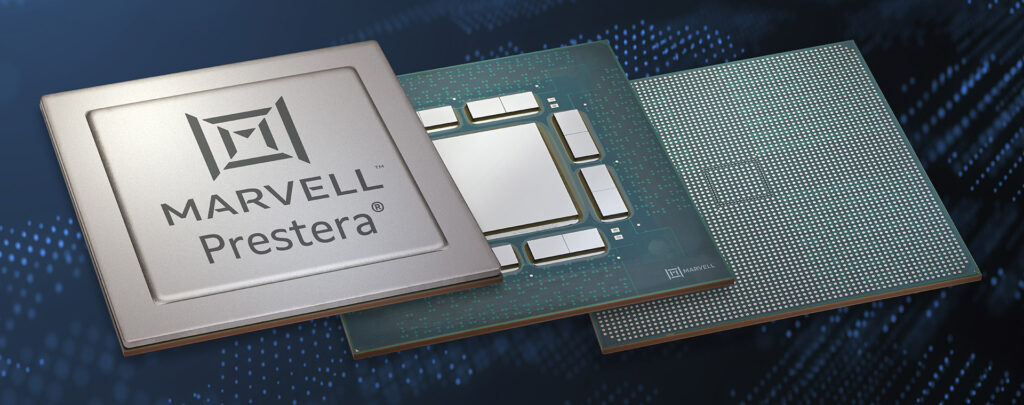 Modular Marvell Network Switch MCM
What’s Driving Main Application Spaces?
First, let’s take a look at different application spaces and how package integration is critical to enable the next-generation product solutions. In the wireless application space, the market can be further subdivided into handheld and infrastructure devices. Handheld devices in this space are driven by ultimate density, memory and RF integration to support power and performance requirements, while achieving reasonable consumer price points. Wireless infrastructure products in support of 5G will drive antenna array with RF integration, and on the baseband side, require a modular approach to enable scalable products that meet power, thermal and cost requirements in a small area. In the datacenter, next-generation products will need next-node performance and power efficiency to keep up with demand. Key drivers here are the insatiable need for memory bandwidth and the switch to scalable compute systems with high chip-to-chip bandwidth. Wired networking products already need more silicon area than can fit in a reticle, along with more bandwidth between chips and off-module. This pushes design toward larger package sizes with lower loss, as well as a huge amount of power coupled with high-bandwidth memory (HBM) integration.
The overarching trend then is to integrate more function (and therefore more silicon) into any given product. This task is especially difficult when many of the different functions don’t necessarily want to reside on the same chip. This includes: IO function, analog and RF content, and DRAM technologies. SoCs simply can’t fit all the content needed into one chip. In addition, IP schedules versus technology readiness aren’t always aligned. For instance, processors for compute applications may be better suited to move to the next node, whereas interface IP, such as SerDes, may not be ready for that next node until perhaps a year later.
How does the package play into this?
All of these requirements mean we as semiconductor solution providers must now get more than Moore out of the package meaning: we need to get more data and more functionality out of the package, while driving more cost out.
As suitable packaging solutions become increasingly complex and expensive, the need to focus on optimized architectures becomes imperative. The result is a balancing act between the cost, area and complexity of the chip versus the package. Spending more on the package may be a wise call if it helps to significantly reduce chip cost (e.g. splitting a large chip in two halves). But the opposite may be true when the package complexity starts overwhelming the product cost, which can now frequently be seen on complex 2.5D products with HBM integration. Therefore, the industry is starting to embrace new packaging and architectural concepts such as modular packages, chiplet design with chip-to-chip interfaces, or KGD integrated packages. An example of this was the announcement of the AMD Epyc 2 Rome chiplet design which marries its 7nm Zen 2 Cores with 14nm I/O die. As articulated in the introductory review by Anton Shilov of AnandTech at the time of its announcement, “Separating CPU chiplets from the I/O die has its advantages because it enables AMD to make the CPU chiplets smaller as physical interfaces (such as DRAM and Infinity Fabric) do not scale that well with shrinks of process technology. Therefore, instead of making CPU chiplets bigger and more expensive to manufacture, AMD decided to incorporate DRAM and some other I/O into a separate chip.”
These new approaches are revolutionizing chip design as we know it. As the industry moves toward modularity, interface IP and package technology must be co-optimized. Interface requirements must be optimized for low power and high efficiency, while enabling a path to communicate with chips from other suppliers. These new packaging and systems designs must also be compatible with industry specs. The package requirements must enable lower loss in the package while also enabling higher data bandwidth (i.e. a larger package, or alternative data transfer through cables, CPO, etc.).
What’s Next for Data Center Packaging and Design?
This is the first in a two-part series about the challenges and exciting breakthroughs happening in systems integration and packaging as the industry moves beyond the traditional Moore’s Law model. In the next segment we will discuss how packaging and deep package expertise are beginning to share center stage with architecture design to create a new sweet spot for integration and next-generation modular design. We will also focus on how these new chip offerings will unleash opportunities specifically in the data center including acceleration, smartNICs, process, security and storage offload. As we embark on this new era of chip design, we will see how next-generation ASICs will help meet the expanding demands of wired networking and Cloud Data Center chip design to power the data center all the way to the network edge.
# # #
1 Moore’s Law, an observation or projection articulated in 1971 stated that the number of transistors in integrated circuit chips would double every two years.
Tags: 112G SerDes, 5G Wireless Infrastructure, 5nm, Acceleration, Cloud Data Center, Network edge, Networking, Offload, prestera, Process, Security, Semiconductor, serdes, SIC, single chip module packaging, smartNICs, storage, Switch, System Integration