



By Abed Mohammad Kamaluddin, Director, Custom Cloud Solutions, Marvell, and Vienna Alexander, Marketing Content Professional, Marvell
For most of the last decade, scaling AI meant scaling compute. If you built faster accelerators and wired enough of them together, the models would follow.
That is no longer the whole picture. Models now run to hundreds of billions of parameters with extensive context windows, and whether an expensive accelerator is working or just waiting comes down to memory: how much you have, how fast you can reach it, and how much time you lose moving data around.
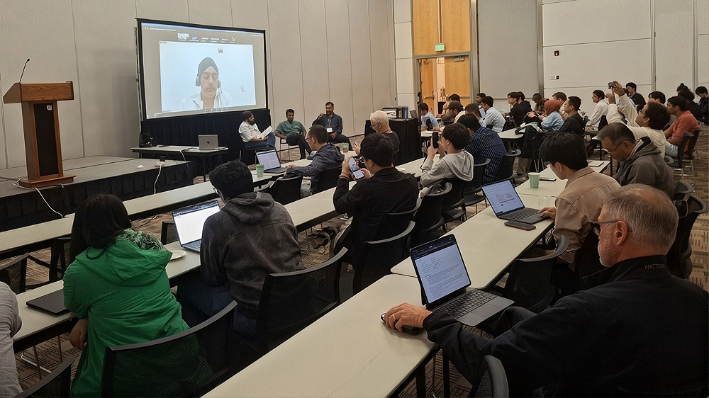
Once memory leaves the server and rides a switched fabric, is it still memory, or has it become a network? This was the central question of MemNetAI, the first workshop on Memory-Semantic Networking for AI-Scale Systems, launched by Marvell with researchers from IIT Hyderabad and IIIT Delhi. Held at ACM SIGCOMM 2026 in Denver and guided by a program committee spanning academia and industry, it brought speakers from Cornell, alongside industry experts and researchers presenting their work, to debate these questions on the bleeding edge of AI infrastructure.
This article is part four in a series on talks delivered at Accelerated Infrastructure for the AI Era, a one-day symposium held by Marvell in April 2024.
Silicon photonics—the technology of manufacturing the hundreds of components required for optical communications with CMOS processes—has been employed to produce coherent optical modules for metro and long-distance communications for years. The increasing bandwidth demands brought on by AI are now opening the door for silicon photonics to come inside data centers to enhance their economics and capabilities.
What’s inside an optical module?
As the previous posts in this series noted, critical semiconductors like digital signal processors (DSPs), transimpedance amplifiers (TIAs) and drivers for producing optical modules have steadily improved in terms of performance and efficiency with each new generation of chips thanks to Moore’s Law and other factors.
The same is not true for optics. Modulators, multiplexers, lenses, waveguides and other devices for managing light impulses have historically been delivered as discrete components.
“Optics pretty much uses piece parts,” said Loi Nguyen, executive vice president and general manager of cloud optics at Marvell. “It is very hard to scale.”
Lasers have been particularly challenging with module developers forced to choose between a wide variety of technologies. Electro-absorption-modulated (EML) lasers are currently the only commercially viable option capable of meeting the 200G per second speed necessary to support AI models. Often used for longer links, EML is the laser of choice for 1.6T optical modules. Not only is fab capacity for EML lasers constrained, but they are also incredibly expensive. Together, these factors make it difficult to scale at the rate needed for AI.
By Radha Nagarajan, SVP and CTO, Optical and Copper Connectivity Business Group
The exponential increase in bandwidth demand will drive continuous innovation in, and deployment of, data movement interconnects for Cloud and Telecom providers. As a result, highly integrated silicon photonics platform solutions are expected to become a key enabling technology for the cloud and telecom market over the next decade.
What Does Highly Integrated Silicon Photonics Platform Mean for the Infrastructure Business?
As speed continues to go up, optical will replace copper as the primary conduit of the digital bits inside Cloud data centers. Marvell is investing heavily in silicon photonics to complement our high-speed CMOS technologies in data center interconnects to accelerate this transition.